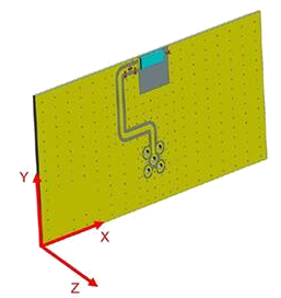
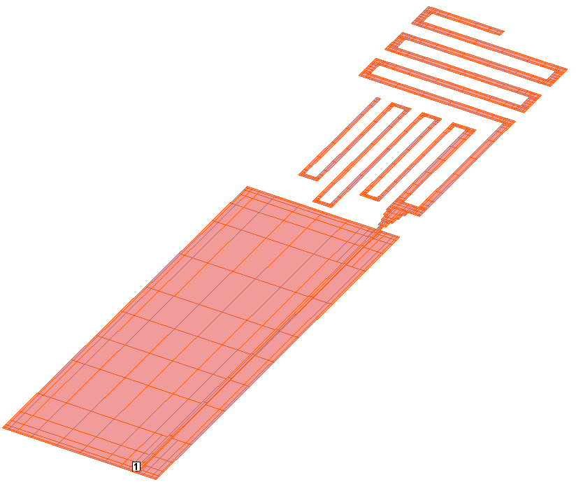
 Who hasn’t considered copying a reference antenna design for their connected product ? It seems efficient, and best of all, totally free ! But guaranteeing that the antenna will perform as expected in your product is likely not as simple as it appears.
Why ? Because your product rarely replicates the same integration environment as the reference design, differences in ground plane size, PCB layout, clearance zones, or the presence of nearby elements such as a battery, screen, or internal cabling can drastically affect RF performance. Even the mere presence of the product's casing can significantly degrade antenna behavior, and with it, your device's overall performance.
Too often, design teams are forced to revisit early development stages during late validation or even during certification, resulting in costly delays and compromised time-to-market.
Every designer strives to build the perfect product, in every respect. But the development of a connected device is always a matter of compromise, whether economic, marketing, technical, or functional.
To reduce the impact of these compromises, or when limited space prevents optimal antenna placement, or simply when enhanced RF performance is required, a custom antenna design is often the most effective solution, especially in high-volume production contexts.
A custom antenna makes the RF link an integral part of the product itself. It can reduce the number of components needed, minimize device size and cost, and most importantly, optimize RF performance, boosting both product reliability and user experience.

